Supporting the below United Nations Sustainable Development Goals:支持以下聯合國可持續發展目標:支持以下联合国可持续发展目标:
Integrated photonics is an emerging branch of photonics in which waveguides and devices are fabricated as an integrated structure onto the surface of a flat substrate, or flat surface. As a result of integration, complex photonic circuits can now process and transmit light in similar ways to how electronic integrated circuits process and transmit electronic signals.
Today, Facebook, Amazon and Google alone run massive cloud computing data centers. As we store and process more information in the cloud, the demands on our wired and wireless networks multiply. Using integrated photonics, the centers will be able to handle greater Terabit-scale data rates of traffic with nanosecond switching speeds, while consuming only half as much power, resulting in a dramatic cost savings.
In this webinar, we will give you an overview on integrated Photonics and discuss the latest of advanced materials for integrated Photonics in Hong Kong.
Rundown
09:00-09:15 Introduction by Moderator Prof. Hon Ki TSANG, IEEE and OSA Fellow, CUHK
09:15-10:00 Overview of Integrated Photonics and its outlook by Prof. John BOWERS
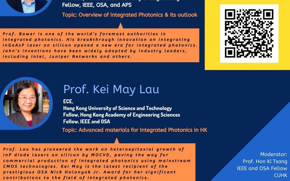
10:00-10:45 Advanced materials for Integrated Photonics in Hong Kong by Prof. Kei May LAU
10:45-11:00 Program Wrap-up and Q&A
Prof. BOWERS is one of the world’s foremost authorities in integrated photonics. His breakthrough innovation on integrating InGaAsP Laser on silicon opened a new era for integrated photonics. John’s inventions have been widely adopted by industry leaders, including Intel, Juniper Networks and others.
Prof. LAU has pioneered the work on heteroepitaxial growth of InP diode lasers on silicon by MOCVD, paving the way for commercial production of integrated photonics using mainstream CMOS technologies. Kei May is the latest recipient of the prestigious OSA Nick Holonyak Jr. Award for her significant contributions to the field of integrated photonics.
