ECE Departmental Seminar - Unlocking the Potential of Gallium Nitride Power Devices
Supporting the below United Nations Sustainable Development Goals:支持以下聯合國可持續發展目標:支持以下联合国可持续发展目标:
Gallium nitride (GaN), with its wide energy gap and versatile heterojunctions, has gained major tractions in power electronics and RF applications. With attractive material properties such as high critical electric field and strong polarization effect, along with the adoption of low-cost scalable Si substrates and Si-compatible manufacturing processes, the GaN high-electron-mobility transistor (HEMT) technology platform offers compelling opportunities for further expansion from integration point of view. Meanwhile, numerous reliability issues need to be addressed for GaN to tap into the lucrative yet more demanding industrial and automotive applications. This talk intends to present some of the latest development in GaN power integration and reliability enhancement.
The development of GaN complementary MOS (CMOS) will also be discussed to illustrate the robustness and expansion capability of the GaN power device technology platform. By exploring the 3rd dimension of the planar GaN power devices, i.e., the space underneath space underneath the GaN epi-structures, a GaN/SiC hybrid field-effect transistor (HyFET) will be illustrated to harness the complementary merits of both GaN and SiC devices.
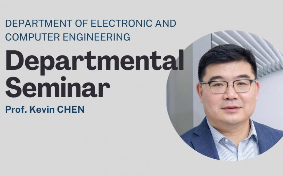
Prof. CHEN is currently a Chair Professor in the Department of Electronic and Computer Engineering. At HKUST, he established the WIde-bandgap Semiconductor Electronics Laboratory (WISE Lab), focusing on technology development of GaN and SiC power and high-frequency devices and ICs. He has led the invention of novel device concepts including composite-channel III-nitride HEMTs, double-heterojunction and double-channel III-nitride HEMTs, self-aligned enhancement-mode III-nitride HEMTs, enhancement-mode MISHFETs and planar integration of E/D-mode AlGaN/GaN HEMT, GaN-based MEMS using GaN-on-Patterned-Silicon (GPS), low-density-drain HEMT (LDD-HEMT), lateral field-effect rectifier, enhanced back barrier HEMT (EBB-HEMT), metal-2DEG tunnel junction FET (TJ-FET), GaN-based HEMTs on modified SOI substrate, photonic-ohmic drain FET (PODFET), GaN/SiC hybrid FET, SiC trench/planar MOSFET (TP-MOS). For these inventions, 11 US patents on GaN device technology have been granted.
Prof. CHEN has led his research group to develop many advanced processing including fluorine plasma treatment and implantation, PEALD-AlN passivation, nitridation interlayer and LPCVD-SiN with interfacial protection layer, etc. His group proposed and demonstrated the GaN smart power IC technology for intelligent high-efficiency power and energy management. Prof. CHEN is a pioneer in developing and understanding the fluorine plasma ion implantation technique for enhancement-mode and normally-off AlGaN/GaN HEMTs and MIS-HEMTs. His group has also developed atomistic process modeling and simulation tools for the fluorine plasma ion implantation technology.
